


scanning electron microscopy

SEM ANALYSIS WITH EDS CAPABILITIES
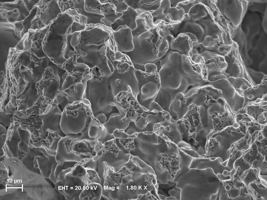
Scanning Electron Microscopy (SEM) is a powerful tool that scans a sample with an electron beam to produce a magnified image for analysis. The highly magnified images provide a powerful and effective micro analysis technique tool in failure analysis, dimensional analysis, contaminant analysis, particle analysis, and reverse engineering. Images produced by a fracture surface are often used to determine the mode and mechanism of failure.
MODERN SEM FACILITIES
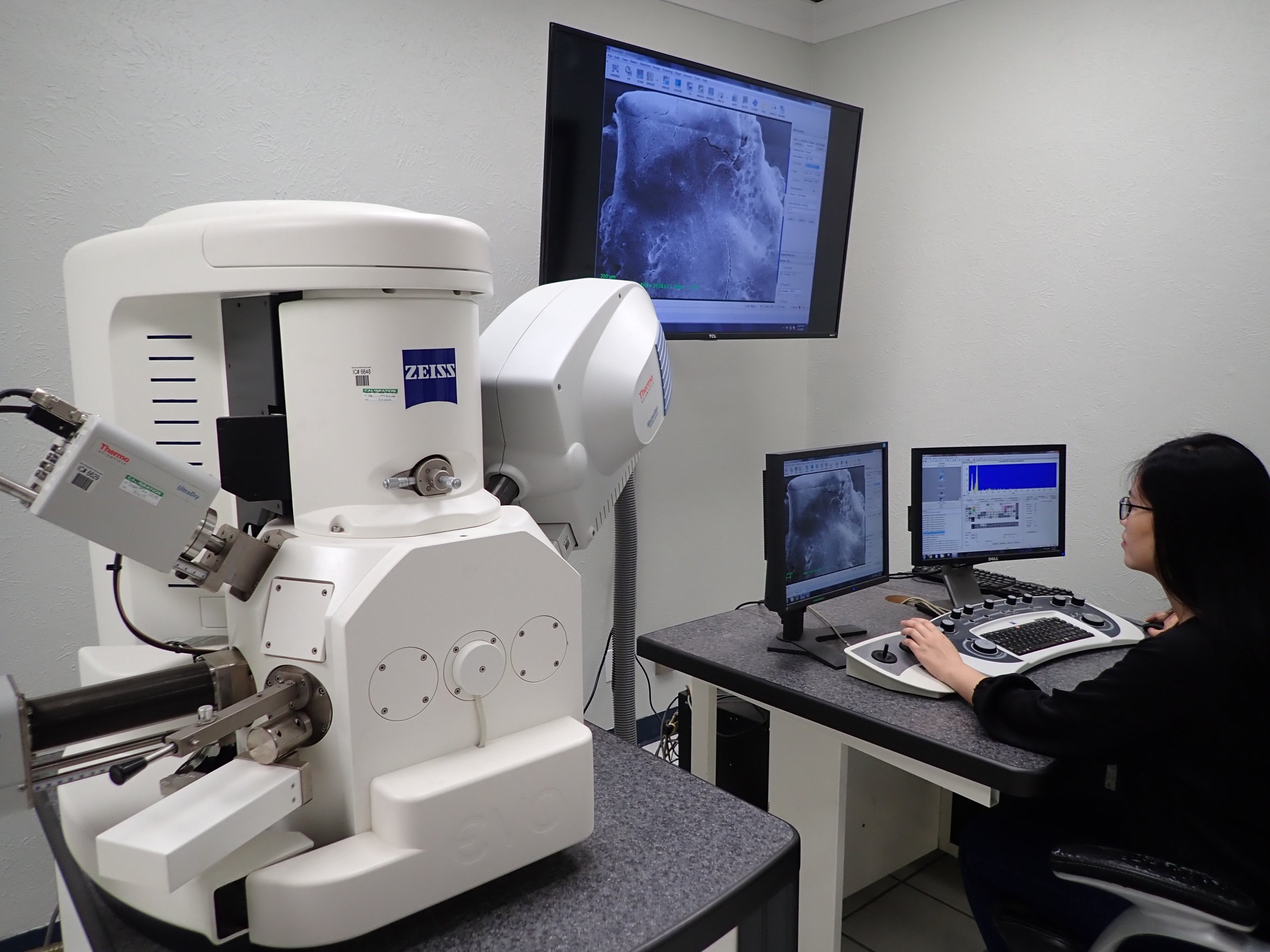
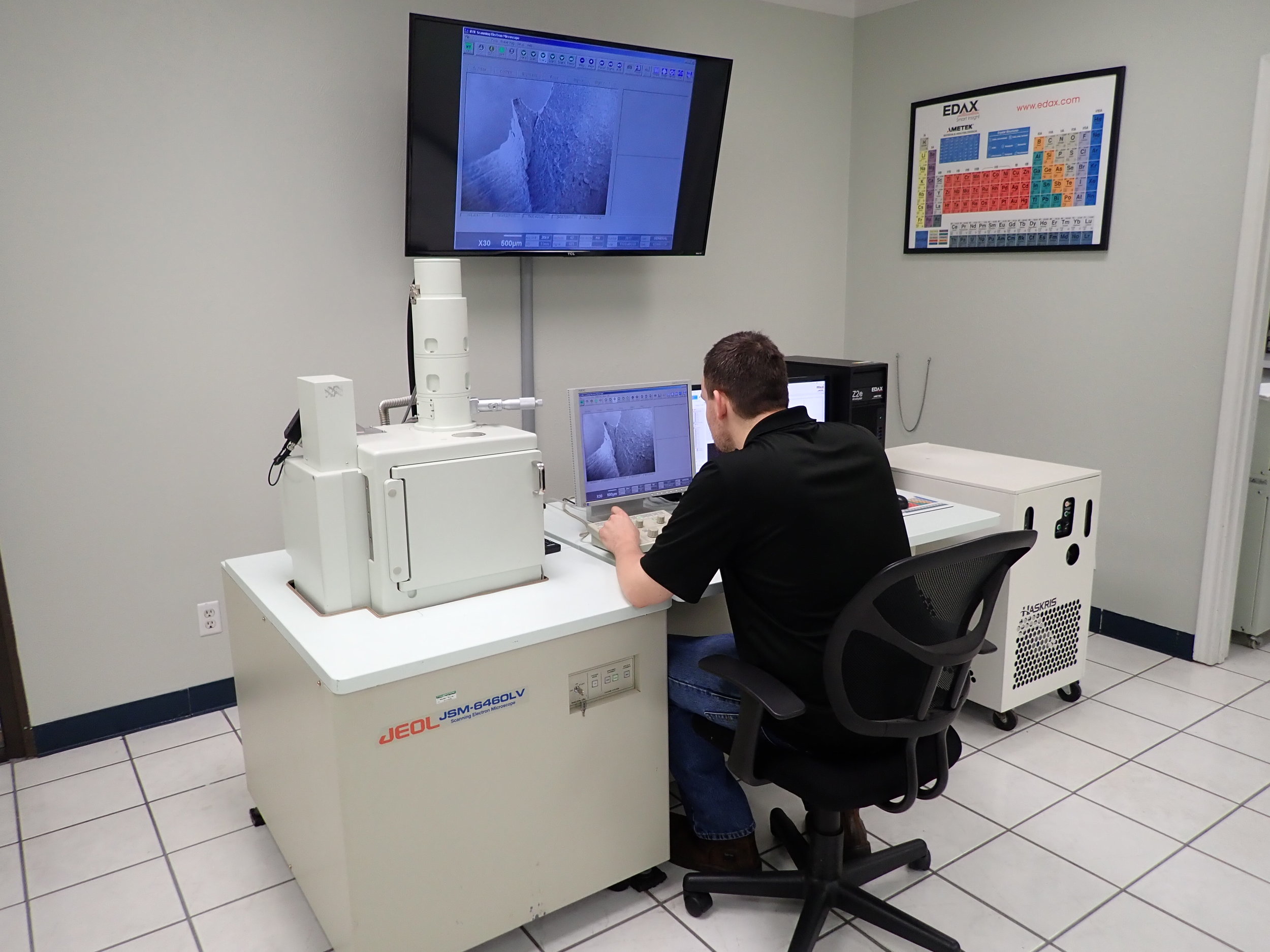
Our surface analysis lab in the Dallas, TX metroplex provides top tier scanning electron microscope services, utilizing Zeiss and Jeol SEMs that include EDAX and Thermo Energy Dispersive X-ray Spectroscopy (EDS) capabilities for chemical composition.
The SEM analysis lab will allow you to view surface features at 5 to 300,000X magnification to provide you with high quality, depth of field images. When used with EDS detectors attached to each SEM, the chemical composition of surface features is quickly attained. While often used for metals and minerals, the IVTS beam lab includes a variable pressure system capable of analyzing non-conductive samples (such as polymers) with minimal preparation.

SEM ANALYSIS REPORTS
Upon completion of your metals testing or analysis, a comprehensive report will be provided with EDS test data, high magnification images, referenced test specification, and interpretation from a materials engineer.
THE SEM ANALYSIS ADVANTAGE
SEM analysis is a proven technique when optical microscopy cannot provide sufficient image resolution or high enough magnification. Analysis by SEM provides a unique depth of field advantage over optical microscopes, allowing the user to focus on irregular fracture surfaces. Our superior instrumentation allows us to provide exemplary service at very competitive prices.
CAPABILITIES
High Magnification Imaging – up to 300,000x
Examination of fractured surfaces
Semi-quantitative chemical analysis by EDS
Evaluation of crystallographic orientation
Low cost chemical and contaminant identification
Analysis of metals, polymers, and minerals
SPECIFICATIONS
ASTM B748 - Metallic Coating Thickness Measurements
ASTM E1508 - EDS Analysis
SAMPLE REQUIREMENTS
Sample Size – up to 8 in. diameter and 3 in. in height